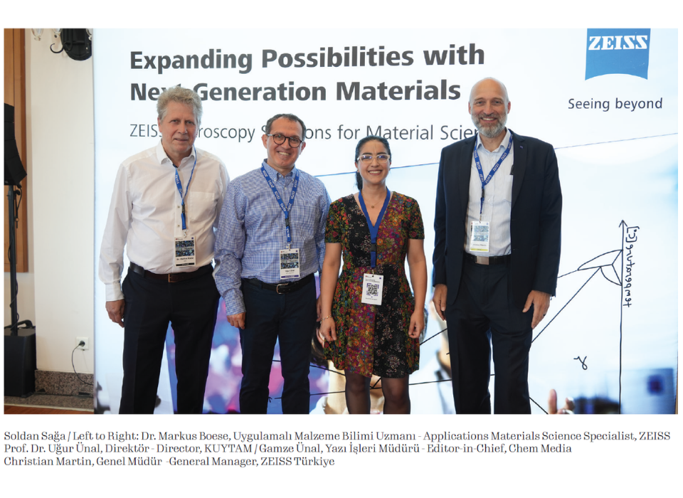
"Microscopy Master Class'26," held on 6-7 May in partnership with Koç University Surface Technologies Research Center (KUYTAM) and ZEISS, brought together academics and industry professionals around the latest innovations in the world of electron microscopy and the nano-level analysis solutions offered by GeminiSEM technology.
Report: Gamze Ünal
Photography: Taner Dalkılıç
Major Collaboration Between KUYTAM and ZEISS: Next-Generation Imaging Technologies Examined at Koç University!
The "Microscopy Master Class'26" organized by Koç University Surface Technologies Research Center (KUYTAM) and ZEISS on 6–7 May brought together the latest innovations in electron microscopy and nano-scale analytical solutions offered by GeminiSEM technology with academics and industry professionals.
KUYTAM – ZEISS Microscopy Master Class'26:
Next-Generation Imaging Technologies Meeting at Koç University
The Microscopy Master Class'26, organized in collaboration between Koç University Surface Technologies Research Center (KUYTAM) and ZEISS, took place on 6–7 May 2026 at Koç University. The event, realized with the vision "Unleash Next-Gen Imaging," brought together academics and industry professionals around the latest innovations in electron microscopy.
Two-Day Intensive Program
The first day (6 May) was held at Founders' Hall. The program, which began with opening remarks by Prof. Dr. Uğur Ünal from Koç University and Christian Martin from ZEISS, continued with theoretical presentations on advanced topics such as ultra-low kV high-resolution SEM, Sweet Spot Imaging, and VR experiences.
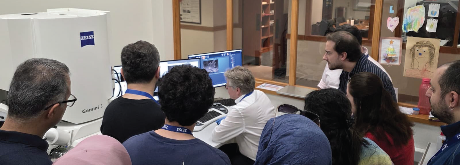
The second day (7 May) was dedicated to practical training at KUYTAM facilities. Participants had the opportunity to work directly on the ZEISS GeminiSEM 560 electron microscope, converting their theoretical knowledge into practice.
Highlighted Topics / The following topics received considerable attention throughout the event:
High-resolution nano-scale imaging with GeminiSEM
Material characterization through advanced EDS analysis
Integration of Oxford Instruments detectors with ZEISS systems and their contribution to research productivity
Analysis of internal sample structure through X-ray microscopy
Nano-structural characterization and analytical solutions
Contribution to Turkey's Research Infrastructure
Following the event, ZEISS Microscopy issued a statement thanking the Koç University KUYTAM team and all participants, emphasizing that they will continue to add value to Turkey's research infrastructure. The Koç University Events Portal can be followed for future events and event summaries.
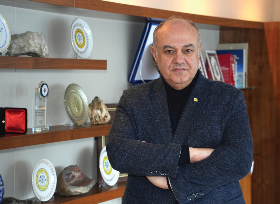
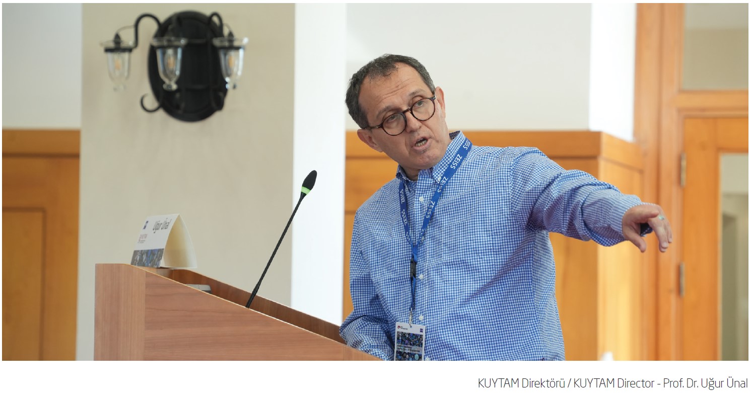 Following the workshop, we spoke with Prof. Dr. Uğur Ünal, Director of KUYTAM, about the role and importance of advanced microscopy techniques in the chemistry industry. In evaluating the new equipment investment and collaboration with ZEISS, Prof. Ünal emphasized that high-resolution surface analyses are indispensable for many critical applications such as catalyst development in surface research.
Could you describe today's workshop?
Today, as Koç University Surface Technologies Research Center, we acquired a new instrument from ZEISS. With the aim of increasing our characterization and analysis capacity, we added one of ZEISS's most advanced models to our facility. We organized a workshop in collaboration with ZEISS to introduce this instrument, which stands out for its high resolution and powerful analytical capacity, and to inform the public about our center.
From a chemistry industry perspective, what is the importance of advanced microscopy techniques?
In the catalytic and surface research we conduct, all reactions take place on the surface. For this reason, understanding the chemical composition, chemical properties, and morphological structure of the surface correctly is of great importance. These characteristics are fundamental factors that directly affect the overall performance of the material in catalytic reactions and all surface-related processes. To access this data, we need high-resolution electron microscopes and analytical electron microscopy systems. Based on the findings we obtain, we perform surface modifications and contribute to the development of application-oriented catalysts.
What do you think about the collaboration between academia and the chemistry industry in Turkey?
At this point, closer collaboration between universities and industrial organizations becomes critically important. One of the most fundamental shortcomings in Turkey is that the relationship between industry and universities has not deepened sufficiently. Although joint projects are conducted, the vast majority of these projects conclude without producing concrete outputs. The relationship between industry and universities needs to be advanced not only on a product-oriented axis but also on technology development and knowledge generation.
Industry, by its nature, tends toward quick and concrete results. However, developing technology, deepening knowledge, and generating original information often carry much greater strategic value. Of the hundreds of projects conducted, only one or two may lay the groundwork for knowledge that truly breaks new ground. Industry's speed-focused expectations create a significant constraint in this area in Turkey. Therefore, industry–university academic collaborations in our country have become a necessity to be advanced to a much higher level.
We thank Artkim Group and Chem Media for their contributions to viewing our event, and we present our gratitude for your interest.
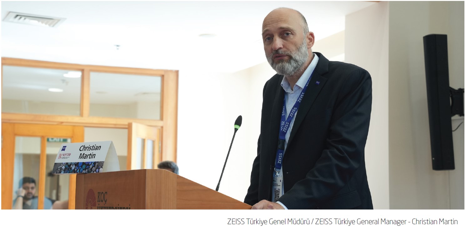 Following his presentation at the Microscopy Master Class'26 event, we conducted an interview with Christian Martin, General Manager of ZEISS Turkey. Drawing attention to the importance of data-driven analytical ecosystems, Martin noted that integrated microscopy solutions increase production efficiency while providing significant advantages in error detection and process optimization.
Chemical manufacturers are under pressure to increase product consistency, process safety, and innovation speed. How do you see advanced electron microscope systems like ZEISS GeminiSEM helping chemistry companies make faster and more confident decisions in areas such as particle characterization, contamination analysis, and failure investigation?
The ZEISS GeminiSEM 560 helps chemistry companies quickly understand micro and nano-scale materials that are sources of many performance and quality issues. For particle characterization, it provides extremely detailed information about particle size, morphology, porosity, and agglomeration behavior. In contamination and failure analysis, integrated analytical tools such as EDS enable rapid identification of foreign particles, inclusions, or process-related defects. Ultra-low kV imaging capability is particularly valuable for sensitive or non-conductive materials because it enables real surface imaging with minimal charging and sample damage. Overall, the system helps accelerate root cause analysis, increase process consistency, and support faster, more reliable decision-making processes.
In light of your international leadership experience spanning Europe, China, North America, and now Turkey, what types of changes are you observing in the digital transformation approach of chemistry industry players? Where can microscopy and analytical workflows create the greatest competitive advantage at this point?
Globally, chemistry companies are progressing from isolated analyses to connected, data-driven workflows. The focus is now on integrating characterization, analytical, and process data to increase efficiency and accelerate innovation. Microscopy systems like ZEISS GeminiSEM are becoming part of larger analytical ecosystems that combine imaging, elemental analysis, automation, and digital data management. The greatest competitive advantage comes from converting microscopy data into actionable process information—that is, helping companies reduce waste, increase repeatability, and optimize production more quickly.
In the Master Class training, ultra-low kV high-resolution SEM for real sample surface imaging is emphasized. Why is having this capability particularly important for coatings and surface professionals when evaluating thin films, adhesion issues, coating defects, and surface-sensitive structures?
In coatings and thin film applications, the most critical information is usually found at the very surface. Ultra-low kV imaging with the ZEISS GeminiSEM 560 allows extremely surface-sensitive analysis without excessive subsurface interference. This enables better evaluation of thin films, nano-scale cracks, adhesion failures, coating defects, and surface contamination. Additionally, it minimizes charging and beam damage on sensitive or non-conductive samples, typically reducing the need for conductive coating during sample preparation. As a result, users can observe material in a state closer to its actual condition and obtain more reliable analytical results.
In the coatings industry, manufacturers often need to combine visual inspection with deeper analytical insights. How does ZEISS help customers move from simply "seeing" a surface defect to "understanding" its "root cause" through integrated microscopy and analytical workflows?
ZEISS helps customers combine high-resolution imaging with integrated analytical workflows to better understand coating defects and failures. With systems like the ZEISS GeminiSEM series, users not only visualize a defect but can also analyze its composition, structure, and origin using tools such as EDS and cross-sectional analysis. This integrated approach allows manufacturers to determine whether problems stem from contamination, processing conditions, material interfaces, or environmental effects; this provides faster troubleshooting and improved product reliability.
Correlative workflows are also truly useful for understanding and combining results. The purpose of correlative microscopy is to enable users to obtain more complete and reliable information from a sample by examining the same area of interest across different microscopes and modalities. One of the greatest advantages of ZEISS correlative workflows is the ability to bridge length scales, from millimeter-scale overview imaging to nanometer-scale ultrastructural analysis. Ultimately, correlative microscopy helps reduce analysis time, increase workflow repeatability, and generate more comprehensive insights from complex materials and structures.
Gallery